
Reliability Testing of Hybrid Bonding Interfaces in 3D-Stacked Memory and Logic
Hybrid bonding has become one of the most important enablers of advanced packaging and heterogeneous integration. It allows memory and logic dies to be joined with extremely fine pitch, low interconnect resistance, and a level of vertical density that traditional micro-bumps cannot match. That technical promise is exciting, but it also raises a hard question: can these interfaces survive real-world operation for years, under heat, stress, and repeated power cycling? Reliability testing is where the answer is found.
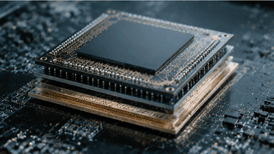
In 3D stacked memory and logic, the hybrid bond interface is not just a connection point. It is the backbone of the entire architecture. If it fails, the whole stack can fail. That makes reliability qualification much more than a checkbox exercise. It is a deep, multi-stage process that must capture mechanical, electrical, thermal, and environmental risks before a product can move confidently into production.
Why Hybrid Bonding Changes the Reliability Conversation
Traditional packaging relied heavily on solder bumps, underfill, and relatively forgiving interconnect geometries. Hybrid bonding replaces that with a far denser interface, typically involving dielectric-to-dielectric bonding and direct metal contact. The result is remarkable performance: lower parasitics, higher bandwidth, better energy efficiency, and a much smaller vertical footprint.
But the interface is also more delicate. The pitch is finer, the alignment tolerance is tighter, and the consequences of small defects are more severe. A particle, void, or slight surface imperfection can compromise an area of the bond that would have been more tolerant in a bump-based package. Reliability testing must therefore probe not only whether the bond works on day one, but whether it continues to work after thousands of thermal cycles, moisture exposures, and mechanical stresses.
That is especially true in 3D stacked memory and logic, where two very different functional blocks are physically tied together. Memory stacks may behave differently from logic dies under thermal load, and the bond interface must accommodate those differences without degradation. Reliability is no longer a package-level issue only; it is a system-level issue hidden inside the stack.
The Stakes in 3D Stacked Memory and Logic

The reason the industry cares so much about hybrid bonding reliability is simple: the business case depends on it. 3D stacked memory and logic architectures promise dramatic gains in bandwidth, latency, and footprint. For AI accelerators, high-performance processors, and advanced memory systems, those gains can be transformative. But they only matter if the interface survives actual product lifetimes.
In memory-on-logic stacks, the bond interface may need to support:
- Very high data throughput over many thousands of connections.
- Continuous thermal stress from active compute below and memory above.
- Long-term stability under voltage, current, and temperature variation.
In logic-on-logic stacks, the demands can be even harsher because both sides may be power-hungry, timing-sensitive, and thermally active. A weak or unstable bond can create timing drift, intermittent faults, or latent reliability failures that are extremely difficult to diagnose after assembly. The interface must therefore be tested like a critical system, not like a passive connector.
What Reliability Testing Must Prove
Reliability testing of hybrid bonding interfaces has to answer several different questions at once. Is the bond mechanically sound? Does it retain electrical continuity? Does it survive heat and humidity? Does it resist degradation over time? Can the package tolerate manufacturing variation without catastrophic yield loss?
The challenge is that these questions are linked. A process that looks electrically perfect may still be mechanically fragile. A bond that survives initial qualification may fail after repeated cycling. A design that appears robust in simulation may prove sensitive to particle contamination or local stress concentrations in real production.
That is why reliability qualification usually includes a broad mix of tests rather than one single stress condition. Hybrid bonding needs to be evaluated from the moment the wafers or dies are prepared through the full product lifetime. The interface must be tested as part of the whole stack, because that is how it behaves in the field.
Key Failure Modes

The most useful reliability programs start by identifying the main failure modes. In hybrid bonding, those typically include:
- Void formation. Small gaps or incomplete contact areas can reduce bond quality and lead to localized stress or electrical opens.
- Particle contamination. Even tiny particles on the bonding surfaces can prevent proper dielectric or metal contact.
- Delamination. The bonded interface may separate under thermal or mechanical stress if adhesion is insufficient.
- Metal interface degradation. Over time, the conductive path can degrade due to diffusion, oxidation, or electromigration-related effects.
- Warp-induced stress. Warpage in large stacks can create misalignment or strain that weakens the interface.
Each of these failure modes can be subtle at first. A package may pass initial electrical test and still contain weak points that only emerge after prolonged stress. That is why reliability testing often combines inspection, accelerated life testing, and electrical monitoring.
The Test Matrix
A serious reliability qualification flow for hybrid bonding interfaces usually includes multiple categories of testing. No single test can capture everything, so the matrix has to be broad and layered.
1. Thermal Cycling
Thermal cycling is one of the most important tests because it simulates the expansion and contraction that occurs during real device operation. As the stack heats up and cools down, different materials expand at different rates. The hybrid bond interface has to absorb that stress without cracking or losing contact.
This test is particularly revealing in 3D memory and logic stacks because the dies often have different heat profiles. Repeated cycling can expose weak adhesion, interface fatigue, and long-term mechanical drift.
2. Temperature-Humidity Bias
Moisture is a persistent threat in advanced packaging. Even a high-quality hybrid bond can degrade if moisture penetrates vulnerable areas or interacts with the materials around the bond. Temperature-humidity-bias testing helps reveal those weaknesses.
This is especially important for products intended for automotive, industrial, or datacenter environments where exposure conditions can be severe and lifetimes long. If the bond survives moisture under electrical bias, confidence in field reliability rises sharply.
3. Power Cycling
Power cycling simulates the repeated turning on and off of the device or the variation in thermal load during operation. This matters because many failure mechanisms appear not under steady state, but under repeated transitions. The interface may gradually fatigue or accumulate microscopic damage after many cycles.
For 3D stacked logic-memory products, power cycling can be especially important because the lower dies may see intense heat while the upper dies remain cooler. That gradient can stress the bond line in ways that are not obvious in simple static tests.
4. Mechanical Stress Testing
Hybrid-bonded stacks must also survive mechanical shocks, vibration, board flex, and handling during assembly and transport. Mechanical stress testing checks whether the interface can tolerate those real-world events without fracture or delamination.
This is a good reminder that a bond can be electrically elegant and still be mechanically vulnerable. Advanced encapsulation must support the bond, not just surround it.
Inspection and Metrology Matter Too
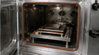
Reliability testing is not only about stressing the device until it fails. It also depends on observing the interface before and after stress. That is where metrology and inspection become essential.
Advanced bonding interfaces may be evaluated with:
- X-ray techniques to detect voids or alignment issues.
- Acoustic or ultrasonic inspection to identify delamination.
- Surface metrology to measure flatness, roughness, and bond quality.
- Electrical continuity tests to validate interconnect integrity.
These tools help build the link between process variation and reliability outcomes. If a certain surface roughness or particle level correlates with early failure, process engineers can adjust cleaning, activation, or alignment parameters before full-scale production. That feedback loop is what turns reliability testing into process improvement.
Why 3D Stacked Memory Is Especially Sensitive
Memory stacks are often the first place where hybrid bonding reliability becomes visible because they demand high density and repeatability. A memory stack may include many repeated interfaces, and a defect in any one bond line can compromise the entire structure. The uniformity requirement is extremely high.
At the same time, memory products are often expected to operate at high bandwidth with low latency and relatively tight timing margins. That means even small interface degradation can show up as performance drift or error-rate growth before catastrophic failure occurs. Reliability testing in memory stacks therefore has to watch not just for open failures, but also for subtle electrical changes over time.
Logic stacks add a different layer of complexity. They often have larger power swings, more dynamic thermal behavior, and stronger demands on timing stability. In those cases, the bond interface must be reliable under both electrical and mechanical stress while preserving performance consistency across the stack’s lifetime.
Interplay with Encapsulation and Materials
Hybrid bonding reliability cannot be separated from the rest of the package. Encapsulation materials, underfill strategies, mold compounds, substrates, and thermal interfaces all influence the bond’s behavior. A great bond can be undermined by surrounding materials that introduce excess stress or moisture sensitivity.
That is why advanced encapsulation plays such a big role. The package must protect the bonded interface while also allowing it to operate within a stable mechanical and thermal environment. Material choices affect:
- CTE mismatch between layers.
- Stress distribution across the stack.
- Moisture ingress and long-term adhesion.
- Heat removal from active dies near the bond line.
In other words, hybrid bonding reliability is not just about the bond itself. It is about the package ecosystem around it. That is a classic heterogeneous integration lesson: the whole is more fragile than the sum of the parts unless the system is co-designed carefully.
Design-for-Reliability Is Becoming Essential
The best reliability programs do not wait until the end of development to ask whether hybrid bonding is robust. They build reliability into the design flow from the beginning. That means:
- Planning for alignment tolerances early in the floorplan.
- Designing dies and stack layouts that minimize stress concentrations.
- Choosing surface prep and bonding conditions that maximize uniform contact.
- Including test structures and monitor dies to track bond quality.
This design-for-reliability mindset is especially important in heterogeneous integration because the package may contain dies from different process nodes, different thermal behaviors, and different design teams. The hybrid bond has to unify all of them into one stable system. If the design assumes perfect conditions, the real package will punish that assumption.
How Qualification Evolves Over Time
Reliability testing is not a one-time event. It is an iterative process that evolves with the product and the process. Early prototypes may require aggressive screening and broad failure analysis. As process maturity improves, the test plan may narrow to focus on the most relevant stress conditions and the most likely failure mechanisms.
The important thing is that qualification evidence accumulates over time. If a hybrid bond interface passes initial lab tests, then pilot line tests, then field-return analysis, confidence grows. Eventually the process may become routine enough that the reliability burden shifts from “prove it works” to “maintain it consistently in production.”
That transition from laboratory curiosity to high-volume confidence is what hybrid bonding is trying to achieve in 3D memory and logic. Reliability testing is the bridge between those two worlds.
The Future of Hybrid Bond Reliability
As hybrid bonding moves toward finer pitches, larger stacks, and more aggressive applications, reliability testing will become even more important. Future challenges may include tighter bond dimensions, more sensitive materials, and higher power densities. At the same time, test methods will likely become more sophisticated, combining simulation, inline inspection, accelerated stress, and predictive analytics.
We may also see more specialized qualification flows depending on the application:
- Memory-focused tests emphasizing repeated thermal and electrical uniformity.
- Logic-focused tests emphasizing power cycling and thermal gradients.
- Automotive and industrial tests emphasizing long-term environmental durability.
The direction is clear. Hybrid bonding is not a temporary trend. It is becoming a core pillar of advanced packaging, and reliability testing is the gatekeeper that determines how broadly it can be deployed.
Conclusion
Reliability testing of hybrid bonding interfaces in 3D stacked memory and logic is one of the most important tasks in advanced packaging today. The interface delivers extraordinary density and performance, but those benefits only matter if the bond survives years of thermal, mechanical, and environmental stress. That is why qualification must be broad, disciplined, and closely tied to process and materials development.
In the world of heterogeneous integration, the hybrid bond is both a technical achievement and a reliability challenge. The companies that learn how to validate it properly will be the ones that move fastest from prototype to production. And as the industry pushes deeper into 3D stacking, the bond interface will remain one of the most important places where performance ambition meets physical reality.
You May Like

Narrowing Spread Between NAND Spot and Contract Prices in 2026 – A Signal
By 2026, one of the most watched metrics in the NAND flash market has started to shift in a subtle but meaningful way: the spread between spot prices and long‑term contract prices is narrowing. For casual observers, this may look like just another incremental change in a notoriously volatile industry. For memory makers, module houses, device OEMs, and data center buyers, however, a tightening gap between spot and contract prices is a signal—a reflection of evolving supply–demand balance, risk perceptions, and strategic behavior on both sides of the market.

Price Divergence Trading Strategies Between NAND Flash and DRAM ETFs
NAND flash and DRAM sit at the core of AI storage and computing power. Both are memory, but they are not the same business. DRAM is main memory—fast, volatile, and central to high‑bandwidth workloads like AI training and inference. NAND is non‑volatile storage—slower than DRAM, but crucial to persistent data and large‑scale object storage. The cycles that drive their pricing and margins overlap, yet they often diverge. That divergence is where trading strategies between NAND and DRAM ETFs become interesting.

China’s HBM Localization Progress: The Catch-Up Pace of CXMT and XMC
China’s drive to localize advanced memory technologies has accelerated over the past several years. High-Bandwidth Memory (HBM) sits near the center of that strategy because it is integral to AI accelerators, high-performance computing (HPC) and other strategic compute platforms. Two domestic players—ChangXin Memory Technologies (CXMT) and XMC (Xianghui Memory, commonly referred to as XMC)—have become focal points in assessing how quickly China can close the gap with international incumbents on HBM die, stacking, and packaging.

Thermal Simulation Challenges and Solutions in 3DIC AI Chip Design
As AI workloads push chips to deliver ever higher compute density, designers are increasingly turning to three‑dimensional integration (3DIC) to stack dies vertically and pack more functionality into limited footprints. While 3DIC architectures unlock significant performance and bandwidth advantages, they also introduce complex thermal behaviors that are far harder to predict and manage than in traditional 2D layouts.

An Attempt at Compiling a Memory+Compute Fusion Thematic Index – A Dual-Track Framework
Most AI investors talk about “compute” as if it were the whole story: GPUs, accelerators, chips, cores. But every one of those cores needs somewhere to read from and write to. Memory and storage define how wide the data highway really is. In practice, AI performance is a fusion of compute and memory, not a solo act. So why do so many indices and ETFs separate them into different silos—one for semiconductors, one for memory, one for data centers—when the actual workloads keep blending them?

Surging Demand for Laser Drilling and Plasma Dicing Equipment in Advanced Packaging
Advanced packaging has become one of the semiconductor industry’s most important growth engines, and it is now pulling a surprising set of process tools into the spotlight. Among the most in-demand are laser drilling and plasma dicing equipment. These machines sit close to the heart of heterogeneous integration, fan-out packaging, wafer thinning, TSV formation, glass substrate processing, and other advanced flows where precision, yield, and throughput matter enormously. As packaging moves from a back-end afterthought to a strategic platform, the equipment used to shape, open, and separate materials has become just as important as the dies themselves.

D2D Interface Bandwidth and Latency Comparison in Chiplet Architectures
Chiplet architecture has turned the package into a real performance battleground. Once multiple dies are placed side by side or stacked within the same advanced package, the quality of the die-to-die, or D2D, interface becomes one of the most important determinants of system behavior. Bandwidth is no longer a nice-to-have metric, and latency is no longer a small implementation detail. Together, they shape whether a chiplet system feels nearly monolithic or frustratingly fragmented.

Stock Selection Logic and Alpha Validation of ESG-Themed Semi ETFs
Semiconductor themed ETFs are no longer just about growth and cycles. A growing subset now layers environmental, social, and governance (ESG) criteria on top of traditional sector exposure. These ESG semi ETFs promise two things at once: access to one of the market’s most powerful secular themes, and alignment with sustainability and governance standards. The pitch is appealing, but it raises two hard questions. First, how exactly are these stocks being selected? Second, does the ESG overlay help, hurt, or leave alpha unchanged?